
Who doesn’t like video cards? No one, we think.
So, we have great pleasure to test and review them; they have evolved so much in the past years and as well the prices have gone up.
Today we test another specimen of the NVIDIA’s 9xx series, this time from EVGA, a SSC GTX 970 ACX 2.0. (04G-P4-2975-KR)
This is the outdated version, it was superseded by the 3975 code which has small upgrades (improved power delivery and a redesigned cooling solution). But that doesn’t mean if you get this one it is a lesser product.
The SSC stands for “Super Superclocked” so let’s see how it performs straight out of the box.
First about EVGA:
EVGA Corporation is an American computer hardware company that produces Nvidia GPU based video cards as well as Intel chipset based motherboards for the consumer and enthusiast market segments. Since 2010, the company has begun adding other computer components to its portfolio, including power supplies, computer cases, and gaming mice. Founded in July 1999.
Based on the philosophy of intelligent innovation, market knowledge, and the real time operation, EVGA continues to identify the need in the market place and providing the solution to that need. By offering product differentiation, 24/7 tech support, a 90 day Step-Up program, and other customer focused programs, EVGA is a clear leader in all categories: etail, retail, distribution, and system builders.
With headquarters in Brea, CA, EVGA’s global coverage includes EVGA GmbH in Munich, EVGA LATAM in Miami, and EVGA Hong Kong.
A top world brand and thus EVGA is a top choice when choosing parts to build a new computer.
Price when reviewed: £ 276.94 - via Amazon.co.uk
EVGA Nvidia GTX 970 SSC ACX Cooling 2.0 4 GB Graphics Card
Presentation
Let’s talk about the Maxwell architecture which composes the GTX 9xx family, being the latest (2nd) iteration to date.
It introduced several new technologies:
Dynamic Super Resolution
It renders the game at a higher resolution and shows it in a lower one, this brings more quality to that lower resolution.
In general DSR works like downsampling, but it has simple user on/off control. Textures will now be sampled at higher resolutions that equates to more pixels being sampled.
Nvidia VXGI (Real-Time-Voxel-Global Illumination)
VXGI is the next step in lighting for gaming and, in simple wording, a new real-time global illumination engine technology. Global illumination is often used in the movie industry to produce CG scenes. VXGI is based on using a 3D structure (Voxels) to capture coverage and lighting information at every point in a scene. This data structure can then be traced during the final stage of rendering to precisely determine the effect of light bouncing around in the scene. VXGI provides improved performance for global illumination. This software algorithm will only work with Maxwell GPUs.
Multi-Frame Sampled Anti-Aliasing(MFAA)
However support for Coverage-Sampling Anti-Aliasing(CSAA) was removed.
It gives the same quality as 4x MSAA but has only the performance costs of 2x MSAA. It is based on a Temporal Synthesis Filter with coverage samples per frame and per pixel
HDMI 2.0 support
HDMI 2.0 is the successor to the HDMI 1.4a/b standard that we pretty much all use in this day and era. The primary reason to bring 2.0 support to Maxwell is that 4K Ultra HD televisions require more bandwidth to operate at their full potential. 4K Ultra HD is four times the resolution of 1080p and therefore UHD needs more throughput to manage that extra data going back and forth
DirectX 12
The DX12 release of DirectX will introduce a number of new features for graphics rendering. Microsoft has disclosed some of these features, at GDC and during NVIDIA’s Editor’s conference. Conservative Raster, discussed earlier in the GI section of this paper, is one such DX graphics feature. Another is Raster Ordered Views (ROVs,) which gives developers control over the ordering pixel shader operations. GM2xx supports both Conservative Raster and ROVs. The new graphics features included in DX12 will be accessible from either DX11 or DX12 so developers will be free to use the new features with either the DX11 or DX12 APIs.
Others include:
VR Direct
Multi-Projection Acceleration
Third Generation Delta Color Compression
Multi-Pixel Programming Sampling
Second generation Maxwell also changed the ROP to memory controller ratio from 8:1 to 16:1.
However, some of the ROPs are generally idle in the GTX 970 because there are not enough enabled SMMs to give them work to do and therefore reduces its maximum fill rate.
Second generation Maxwell also has up to 4 SMM units per GPC, compared to 5 SMM units per GPC.
GM204 supports CUDA Compute Capability 5.2 compared to 5.0 on GM107/GM108 GPUs, 3.5 on GK110/GK208 GPUs and 3.0 on GK10x GPUs.
Maxwell second generation has an upgraded NVENC which supports HEVC encoding and adds support for H.264 encoding resolutions at 1440p/60FPS & 4K/60FPS compared to NVENC on Maxwell first generation GM10x GPUs which only supported H.264 1080p/60FPS encoding.
Moving to the the GTX 970.
GM204 is the GPU name for the GTX 970 which has 5.2 billion transistors, on a 398mm² die size.
Then 1664 CUDA/Shader/Stream processors are used, there are 128 CUDA cores (shader processors) per cluster (SMM), 16 SMM, 16 Geometry units, 104 Texture units, 56 ROP units, and a 256-bit GDDR5.
Regarding frequencies we have:
GPU Boost Clock : 1342 MHz
GPU Base Clock : 1190 MHz
For a better view, here it is compared with others and all the quick specs.
And EVGA’s propietary cooling solution the EVGA ACX 2.0
With optimized Swept fan blades, double ball bearings and an extreme low power motor, EVGA ACX 2.0 delivers more air flow with less power, unlocking additional power for the GPU.
Before we go further let’s explore the controversy with the GTX 970.
Via Anandtech which presents it in depth.
http://www.anandtech.com/show/8935/geforce-gtx-970-correcting-the-specs-exploring-memory-allocation
In brief, various GTX 970 owners had observed that the GTX 970 was prone to topping out its reported VRAM allocation at 3.5GB rather than 4GB, and that meanwhile the GTX 980 was reaching 4GB allocated in similar circumstances. All of this was at odds with what we thought we knew about the cards and the underlying GM204 GPU, as the two cards were believed to have identical memory subsystems.
In their statement, NVIDIA confirmed that this unusual behavior existed, and that it was due to the GTX 970 possessing “fewer crossbar resources to the memory system” than the GTX 980. Furthermore due to this, the VRAM on the GTX 970 was segmented in a way it’s not on the GTX 980, with 3.5GB of the 4GB serving as one high priority segment, and the final 512MB serving as a low priority segment. Which leads to the reported performance degradation when an application needs to access more than 3.5GB. The rest of NVIDIA’s statement then focused on performance, and why they believed this design would not have a significant performance impact versus a GTX 980-style non-segmented memory structure.
When the GTX 980 and GTX 970 were released, NVIDIA provided the above original specifications for the two cards. The launch GTX 900 GPUs would be a standard full/die-harvested card pair, with the GTX 980 using a fully enabled GM204 GPU, while the GTX 970 would be using a die-harvested GPU where one or more SMMs had failed. As a result of this the big differences between the GTX 980 and GTX 970 would be a minor clockspeed difference, the disabling of 3 (of 16) SMMs, and a resulting reduction in power consumption. Most important for the conversation at hand, we were told that both possessed identical memory subsystems: 4GB of 7GHz GDDR5 on a 256-bit bus, split amongst 4 ROP/memory controller partitions. All 4 partitions would be fully active on the GTX 970, with 2MB of L2 cache and 64 ROPs available.
This, as it turns out, was incorrect.
As part of our discussion with NVIDIA, they laid out the fact that the original published specifications for the GTX 970 were wrong, and as a result the “unusual” behavior that users had been seeing from the GTX 970 was in fact expected behavior for a card configured as the GTX 970 was. To get straight to the point then, NVIDIA’s original publication of the ROP/memory controller subsystem was wrong; GTX 970 has a 256-bit memory bus, but 1 of the 4 ROP/memory controller partitions was partially disabled, not fully enabled like we were originally told. As a result GTX 970 only has 56 of 64 ROPs and 1.75MB of 2MB of L2 cache enabled. The memory controllers themselves remain unchanged, with all four controllers active and driving 4GB of VRAM over a combined 256-bit memory bus.
This revelation significantly alters how we perceive the performance of the GTX 970 in certain situations, and is the missing piece of the puzzle in understanding the memory allocation issues that originally brought all of this to light. The ability to “partially disable” a ROP/memory controller partition is new to Maxwell, and we’ll fully explore how that works in a moment, but the important part to take away is that the ROP/MC layout on the GTX 970 is not fully enabled like the GTX 980, and as a result will not behave identically to the GTX 980. All of the behavior from the GTX 970 we’ve seen in light of this correction now makes sense, and it is immediately clear that this is not a hardware or software bug in GTX 970, but rather the planned/intentional behavior of the product.
So the memory is split in two segments of 3.5 GB and 512 MB, with a memory bandwidth of 196 GB/s and 28 GB/s, respectively.
The biggest and most painful question about all of this then is how did this happen? How did we get fed incorrect specifications? NVIDIA’s explanation, in a nutshell, is that this was completely accidental and that all of this stems from assumptions made by NVIDIA’s technical marketing team.
Ok, so much for the technical specs and the controversy, let’s see it in hand.
Packaging and content
First we have the box, which you can tell but is small compared to a regular GTX 970, foretelling that this is a very compact video card. On the front and all the information you need, with highlights such as DX12, G-Sync, the SSC so you know it is the Super Superclocked model and the proprietary cooling the ACX 2.0.
On the back we got a more detailed presentation regarding aspects like architecture, ports, technologies etc.
And on the sides more ..marketing.
Inside, we see that EVGA takes a different approach regarding packaging - a clear plastic enclosure.
After removing the accessories, we have the card itself at the epicenter.
Let’s get these out of the way while we are at it.
- 6x Booklets/Fliers
- 2x 4pin MOLEX to 6 pin adapters - in a very nice EVGA bag
- 1x DVI-VGA adapter
- 1X EVGA sticker badge
And finally the card.
Very small just at 241 mm long and no higher than the PCI-E bracket thus perfect for a small form factor build.
Subtle logos on the fan’s hub, the ACX 2.0 on the edge and an overall clean design.
On the back, no included backplate unfortunately, but you can get it separately.
The highlight here is the Samsung VRAMs which should offer better overclocking headroom.
On the top the regular SLI connectors and the 2x 6 pin PCI-E plugs to fuel which are on a median location.
Then the SSC and more branding. Flip it, nothing of interest besides the PCI-E 3.0 connector.
Moving to the back, we have the following display connectors:
- 1x Display Ports 1.2
- 1x HDMI 2.0 @ 4K/60fps
- 1x DVI-D
- 1x DVD-I
And let’s give it a perspective of the compactness we were talking about, compared to other video cards.
From top to bottom:
- MSI 9800 GX2 - 267 mm long
- MSI GTX 760 Twin Frozr IV - 260 mm long
- EVGA GTX 970 SSC ACX 2.0 - 241 mm long
Testing methodology
Hardware used:
Processor: Intel i7 2700k @ 3.5 GHz - Sandy Bridge 32nm, HT and Turbo Boost Enabled up to 3.9 GHz
CPU cooler: Stock Intel
Motherboard: MSI mITX B75IA-E33
RAM: 16 GB DDR3L Crucial Tactical VLP 1600 Mhz
SSD : Samsung 840 Pro 128 GB
Case: Fractal Design Core 1000
Case Fans: 1x 120 mm Fractal Design
PSU: Corsair CX 600W 40A
Display: Samsung 32″ FHD TV LED 100 Hz - UE32F5000
Sound Meter: Pyle PSPL01 – positioned 1 meter from the case, (we will include +/- 2-3 % margin for error) with ambient noise level of 25-30 dB/A
Power consumption: measured via our wall monitor adapter: Prodigit 2000MU
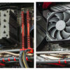
The card installed:
Software
- Windows 7 Ultimate x64 SP1
- NVIDIA GeForce 359.06 WHQL
- GPU-Z v0.8.1
- MSI Afterburner 4.11 - to record the FPS and monitor load/temperatures plus OC, with a room temperature of 20 degrees C.
- Valley Benchmark 1.0
- All games and benchmarks set at 1920 x 1080 resolution with maximum settings applied, V-Sync oFF
Results
The numbers speak for themselves.
Again, these are MAXIMUM settings applied including the high demanding AA and special ones in all the games.
Temperatures
- Desktop idle with the fans OFF: 37 degrees C
- Full gaming load @ The Witcher 3 @ auto % rpm : 74 degrees C
Excellent numbers.
Noise output
At 1450 rpm in full load gaming in Witcher 3, nothing, we are talking about room ambient noise ~ 31 dB/A so maximum points. In idle with the fans OFF, of course there is nothing to record or to hear.
Power consumption
System in IDLE = 41.3 Watts
System Wattage with GPU in FULL Gaming Stress = 265 Watts
Overclock
Using MSI Afterburner, we set the power limit to 110 %.
And managed to obtain a good 110 MHz to the base clock core thus having in the end a dead on 1300 MHz.
That’s ~ 10 % increase.
Then regarding the boost values we managed 1452 MHz with peaks of 1475 MHz under full gaming load.
Maxwell does OC very well.
The we manged to OC the Samsung memories to 7.9 GHz ! That’s 11 % increase !
Stable numbers, all with stock voltages.
And these are the results.
Conclusion
A great overall solution from EVGA with their SSC iteration, it stays cool, great OC, small footprint.
The only negative we found is our sample had bad coil noise, but used within a computer case, it shouldn’t be that bad.
The good:
+ Excellent performance
+ Very quiet and very good thermals
+ One of the best OC from factory at 1342 MHz
+ Good overclocker and a big plus from the Samsung VRAMs
+ High build quality
+ Very small overall dimensions, great for SFF builds
+ Low TDP and power consumption
The bad:
- Disturbing coil noise if used on an opened bench setup
- No backplate, although the is a separate option to buy one
- The 3.5 GB / 0.5 fiasco, but that’s NVIDIA’s fault, not EVGA’s.
Glob3trotters “Great Choice” Award - 4 out of 5