
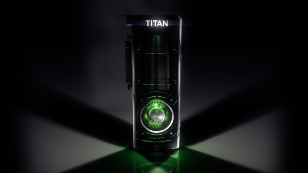
The NVIDIA Geforce GTX TITAN X has just been unveiled at Epic Games GDC 2015 conference.
To be honest, we were not expecting this card to surface so soon – but the surprise is a very pleasant one.
Ladies and gentlemen, rocking 8 Billion transistors, the full fledged big daddy GM200 Maxwell core and 12 GB of graphics memory: The NVIDIA Geforce GTX TITAN X.
Nvidia teases the Nvidia Geforce GTX TITAN X at GDC 2015
You might remember the GM200 leak from a few weeks back and the fact that we know its specifications as well.
Even though that was most likely a Quadro M6000 part the TITAN-X will most probably have the same basic specs, with a slight chance of Nvidia introducing a cut die initially.
The full un-cut GM200 has a 384-bit bus, 12GB of vRAM and 3072 CUDA Cores (which translates to 24 SMM).
Given below is a screenshot of the actual tease.
As for the chip, the GM200 is a massive die measuring at around 600mm2, whereas Kepler GK110 had a die of 561mm2 .
The more surprising thing about this launch is that NVIDIA is now launching their flagship chip faster than ever as compared to Kepler generation which had to wait for a year to see the launch of GK110 (GTX Titan). In only eight month time difference since September, NVIDIA has announced their next flagship entry to consumers and professionals with an absolute beast of memory and compute performance.

NVIDIA GeForce GTX Titan X “Initial” Specifications:
| NVIDIA GeForce GTX Titan X | NVIDIA GeForce GTX Titan Black | NVIDIA GeForce GTX 980 | NVIDIA GeForce GTX 970 | NVIDIA GeForce GTX 960 | |
| GPU Architecture | Maxwell | Kepler | Maxwell | Maxwell | Maxwell |
| GPU Name | GM200 | GK110 | GM204 | GM204 | GM206 |
| Die Size | ~600mm2 | 561mm2 | 398mm2 | 398mm2 | 228mm2 |
| Process | 28nm | 28nm | 28nm | 28nm | 28nm |
| CUDA Cores | 3072? | 2880 | 2048 | 1664 | 1024 |
| Texture Units | TBA | 240 | 128 | 104 | 64 |
| Raster Devices | TBA | 48 | 64 | 64 | 32 |
| Clock Speed | TBA | 889 MHz | 1126 MHz | 1051 MHz | 1127 MHz |
| Boost Clock | TBA | 980 MHz | 1216 MHz | 1178 MHz | 1178 MHz |
| VRAM | 12 GB GDDR5 | 6 GB GDDR5 | 4 GB GDDR5 | 4 GB GDDR5 | 2 GB GDDR5 |
| Memory Bus | 384-bit | 384-bit | 256-bit | 256-bit | 128-bit |
| Memory Clock | 7.0 GHz? | 7.0 GHz | 7.0 GHz | 7.0 GHz | 7.0 GHz |
| Memory Bandwidth | 336.0 GB/s | 336.0 GB/s | 224.0 GB/s | 224.0 GB/s | 112.0 GB/s |
| TDP | 225-250W | 250W | 165W | 145W | 120W |
| Power Connectors | 8+6 Pin | 8+6 Pin | Two 6-Pin | Two 6-Pin | One 6-Pin |
| Price | $999-$1349 US? | $999 US | $549 US | $329 US | $199 US |


